We focus on the investigation of topology, morphology, chemical and phase composition and on the determination of crystallographic orientation.
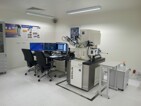
The electron microscopy and microanalysis team has a scanning electron microscope, which is equipped with several types of detectors - a "classic Everhart-Thornley" detector suitable for topographical representation of the sample surface, as well as a so-called in-lens secondary electron detector designed for high-resolution images (representation of nano-objects ), an energy-selective backscattered electron detector (EsB), which is suitable for material contrast imaging, and an angle-selective backscattered electron detector (AsB4) for crystallographic contrast imaging. The last detector for imaging is a segment detector for transmission electrons.
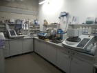
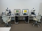
Furthermore, the microscope is equipped with two spectrometrs and one microanalytical detector - an energy dispersive spcectrometer (EDS), a wave dispersive spcectrometer (WDS) - intended for chemical microanalysis, and detector of diffracted backscattered electrons for determining the crystallographic orientation and phase composition of the material. We also have equipment for correlative microscopy, where we can analyze the same spot on the sample with a stereomicroscope with 3D imaging, a polarizing microscope and a scanning electron microscope. The laboratory is equipped with devices for the preparation of polished sections, thin sections and samples for electron transmission microscopy.
We perform both service and experimental measurements.
We arrange a complete material analysis - we determine surface morphology, particle morphology, chemical composition and determine the crystal structure of materials.
We prepare samples for optical and electron microscopy (transmission and scanning).
We perform qualitative and quantitative analysis of the chemical composition of samples using X-ray microanalysis (EDS/WDS).
We determine the phase composition of materials and structure, crystal orientation and phase composition of materials using EBSD.
We make 3D photomicrographs on an optical microscope.
We measure on a polarizing microscope in transmitted and reflected light.
Scanning Electron Microscope with Schottky cathode FEG SEM Merlin, Energy Dispersive Spectrometer (EDS), Wave Dispersive Spectrometer (WDS), Electron Backscattered Diffraction (EBSD), Scanning Transmission Detector (STEM).
Detailed micro / nano analysis of various types of materials. The laboratory has complete equipment for preparing samples for both electron and optical microscopy. The laboratory is focused on investigating the topology, morphology, chemical, structural and phase composition of materials, or determining their crystal orientation.